Chip Annotations
Disclaimer
The annotations are based on rather sparse official technical information, a lot of unofficial information, educated guesses based on observed/benchmarked performance characteristics and also plain old guesses out of thin air.
Some of these annotations are also quite obviously wrong and outdated, take anything on this page as "quite likely wrong".
Simpler file browser.
Intel ArrowLake Architecture
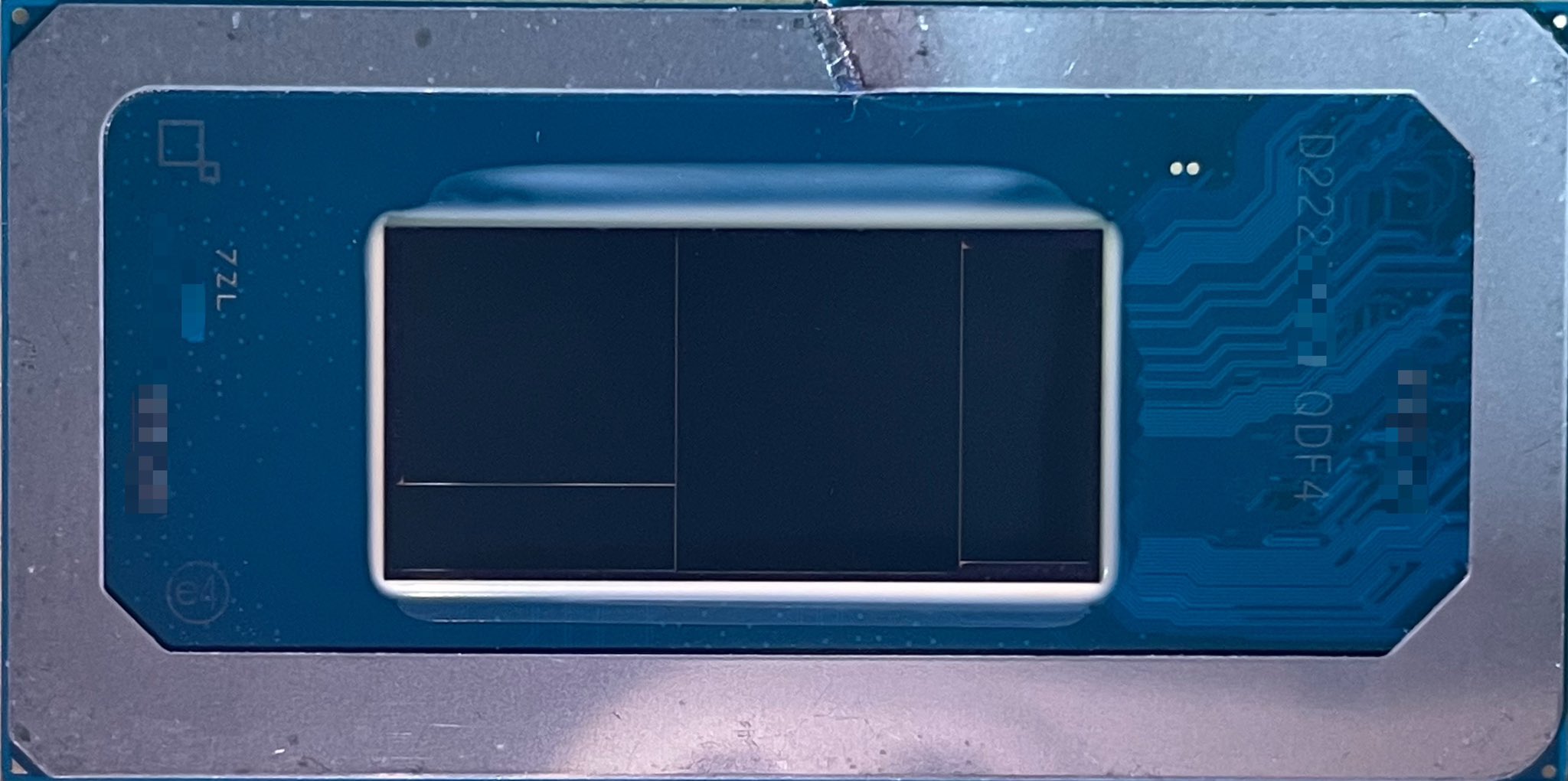
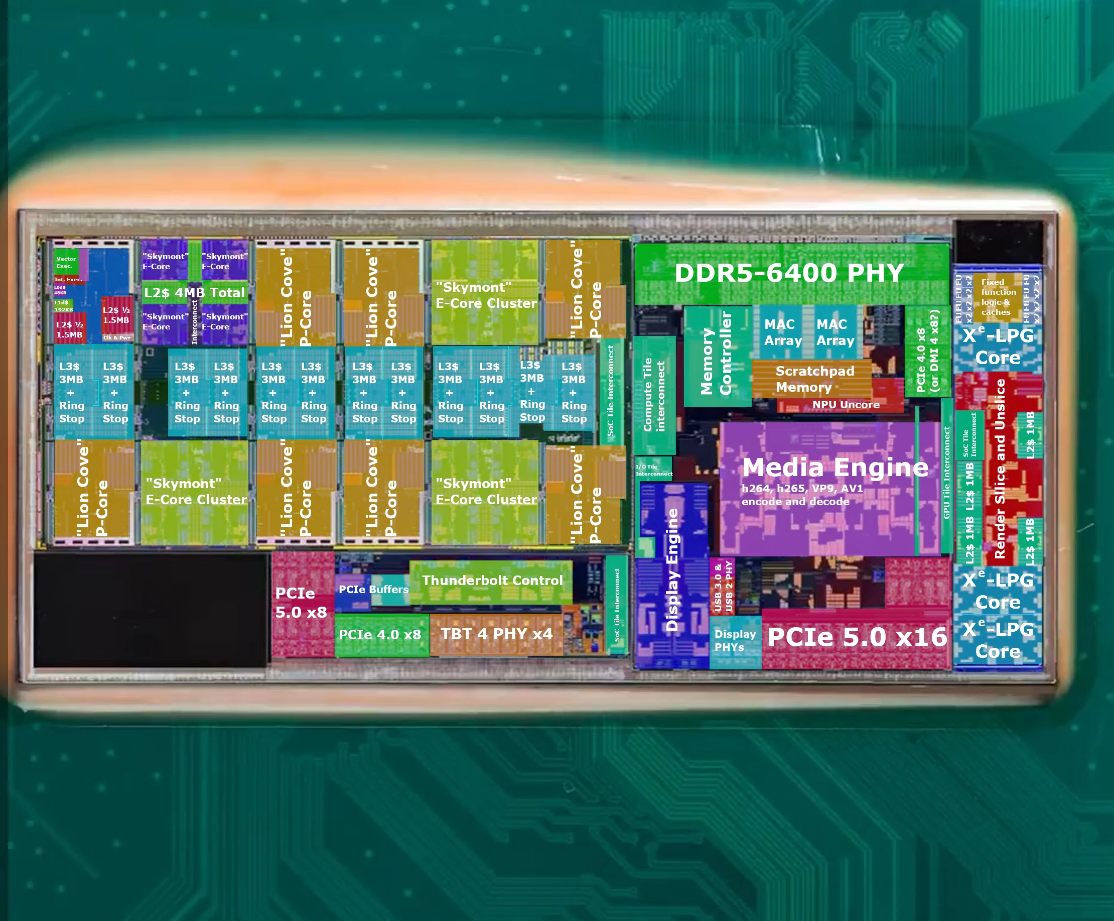 ArrowLake-S
The ArrowLake-S four-chiplet multi-chip was used for the desktop and mobile HX series of the second generation Intel Core Ultra products.
CPU: 8 LionCove P-cores and 16 Skymont E-cores
GPU: 4 Xe-LPG Cores (512 SIMD lanes)
Memory: 128 bit DDR5-6400 memory controller supporting CUDIMMs
IO: 20 PCIe 5.0 lanes and 4 PCIe 4.0 lanes (active on ARL-S)
Annotated View (2220x1834) Download (442.09 kiB)
Original View (2220x1834) Download (363.14 kiB)
Original Source: 普普通通Tony大叔 on bilibili, reposted by HXL (9550pro) on Twitter.
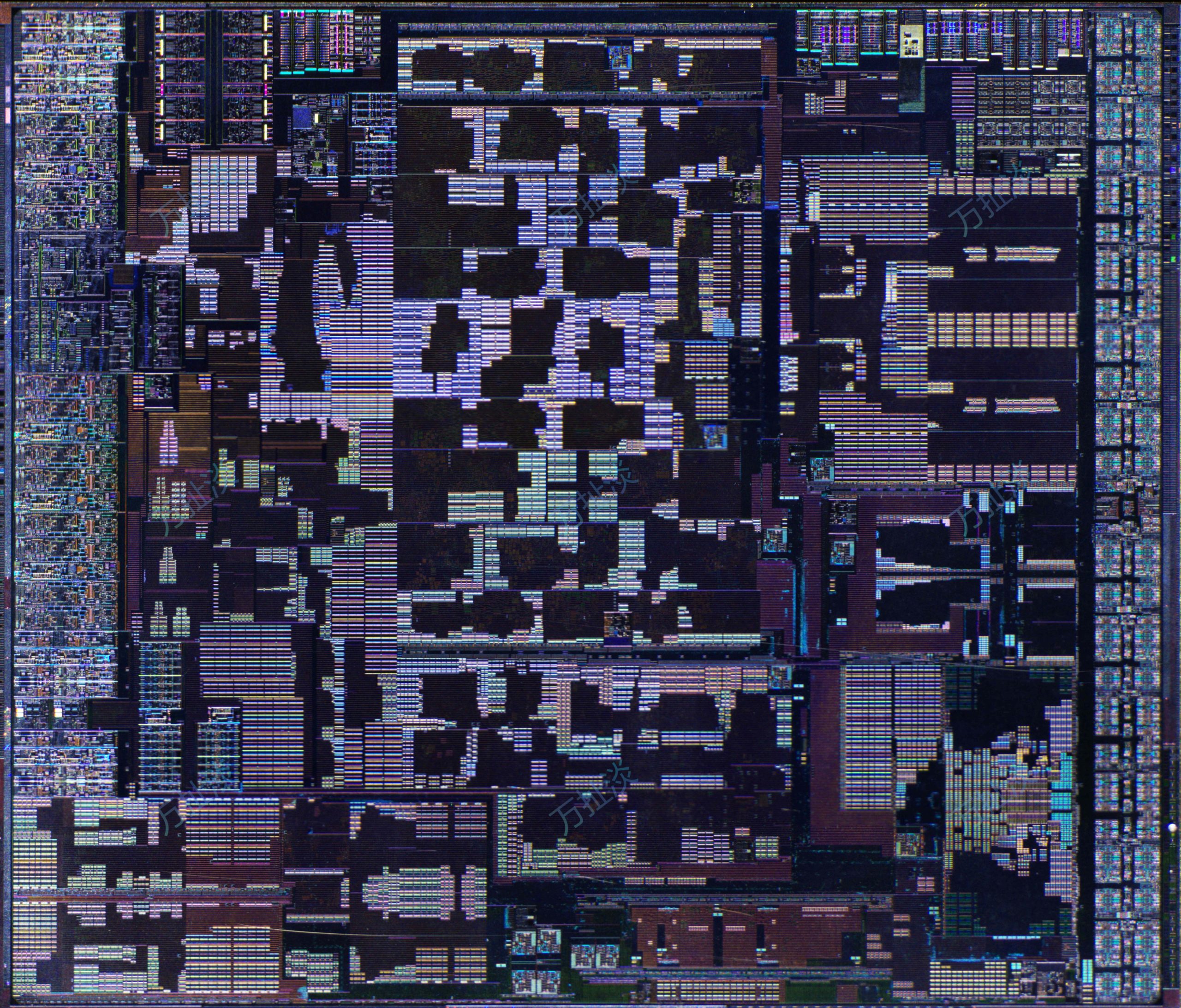
Intel LunarLake Architecture
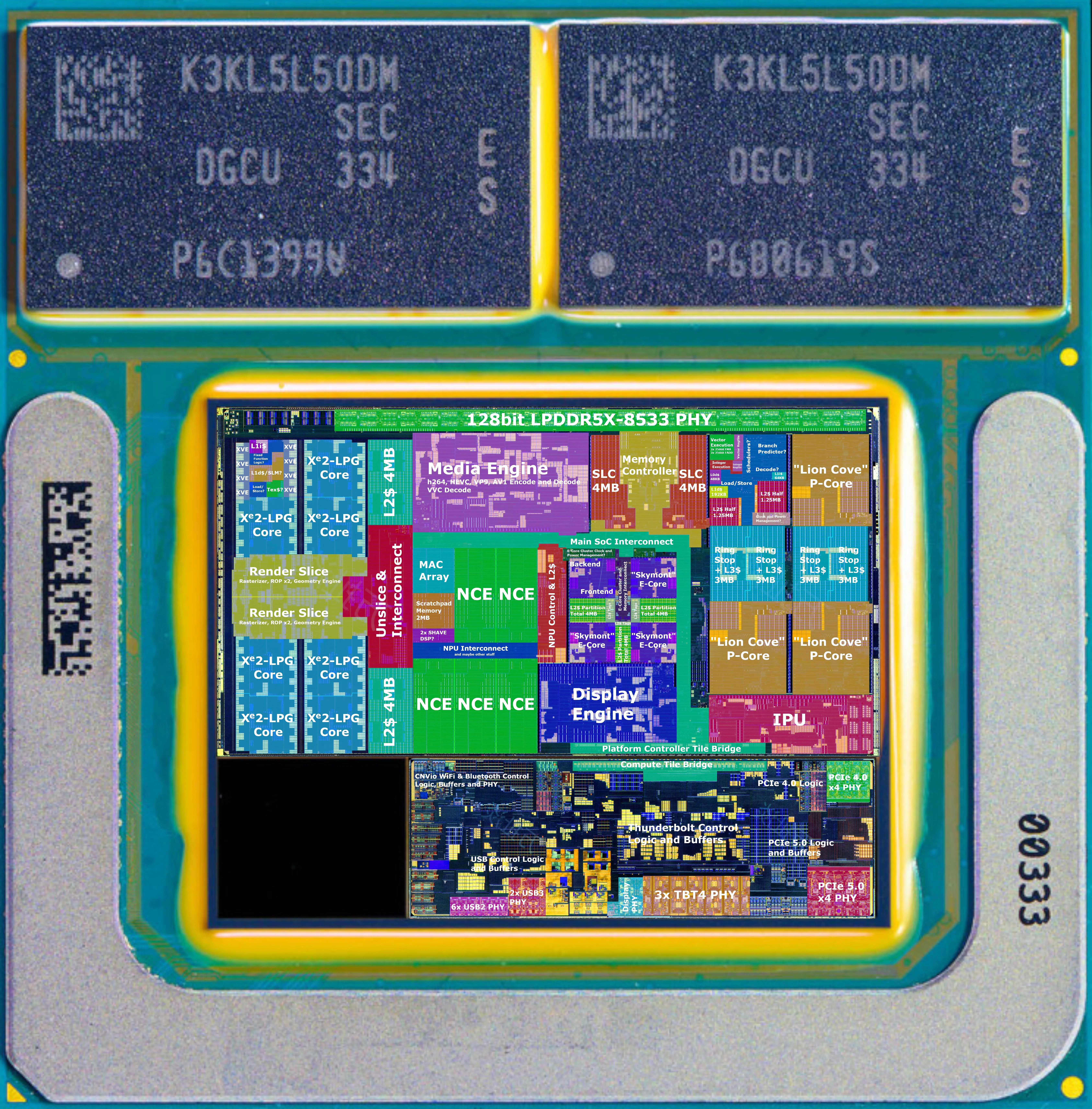 LunarLake-MX
The LunarLake-MX two-chiplet multi-chip was used for the V-Series of the second generation Intel Core Ultra products for premium thin and light laptops.
CPU: 4 LionCove P-cores and 4 Skymont E-cores
GPU: 8 Xe2-LPG Cores (1024 SIMD lanes)
Memory: 128 bit LPDDR5X-8533 memory controller (16 or 32GB on-package)
IO: 4 PCIe 5.0 lanes and 4 PCIe 4.0 lanes
Annotated View (6742x6850) Download (2.68 MiB)
Original Source: GeekerWan and 万扯淡, provided by Kurnal.
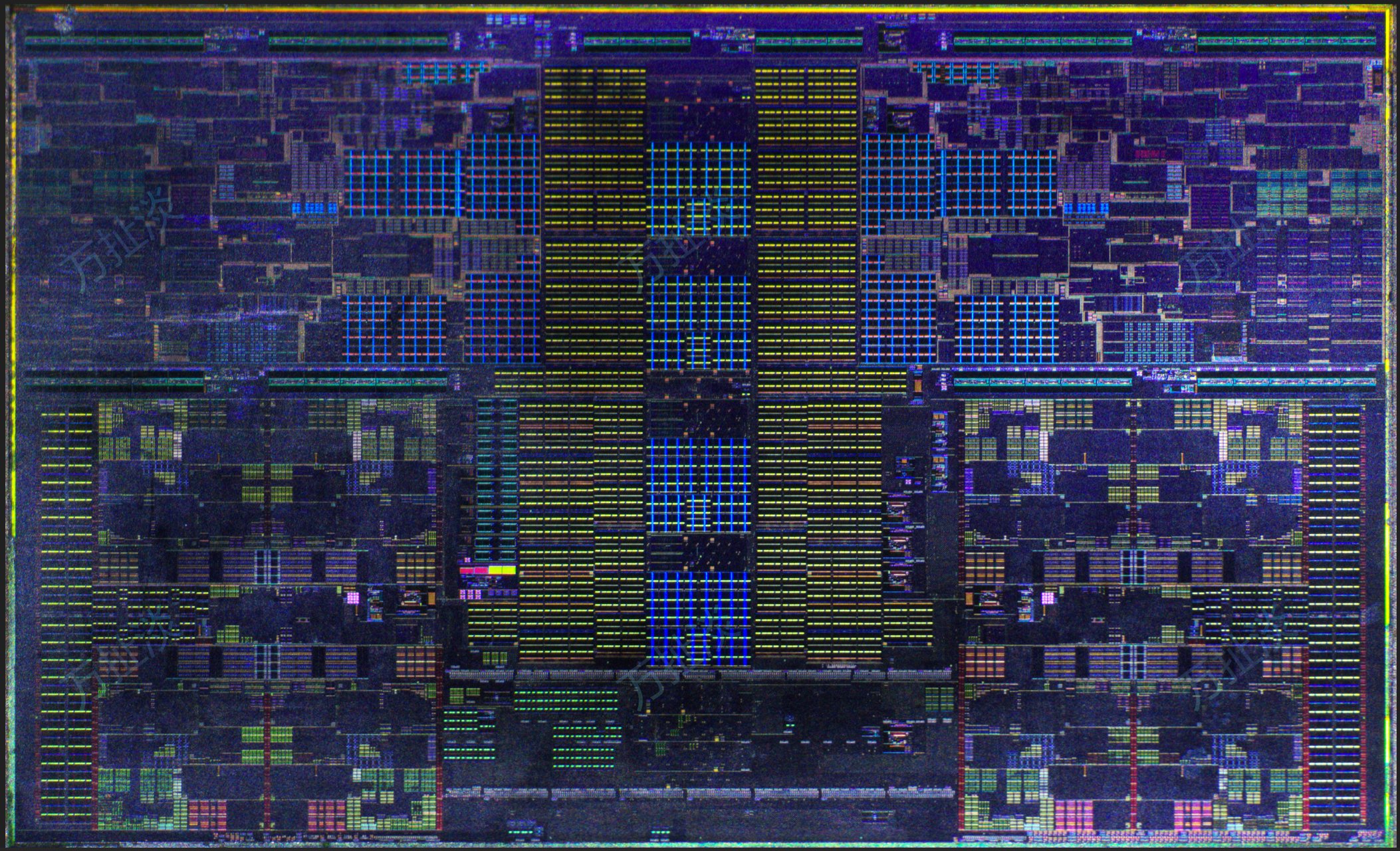
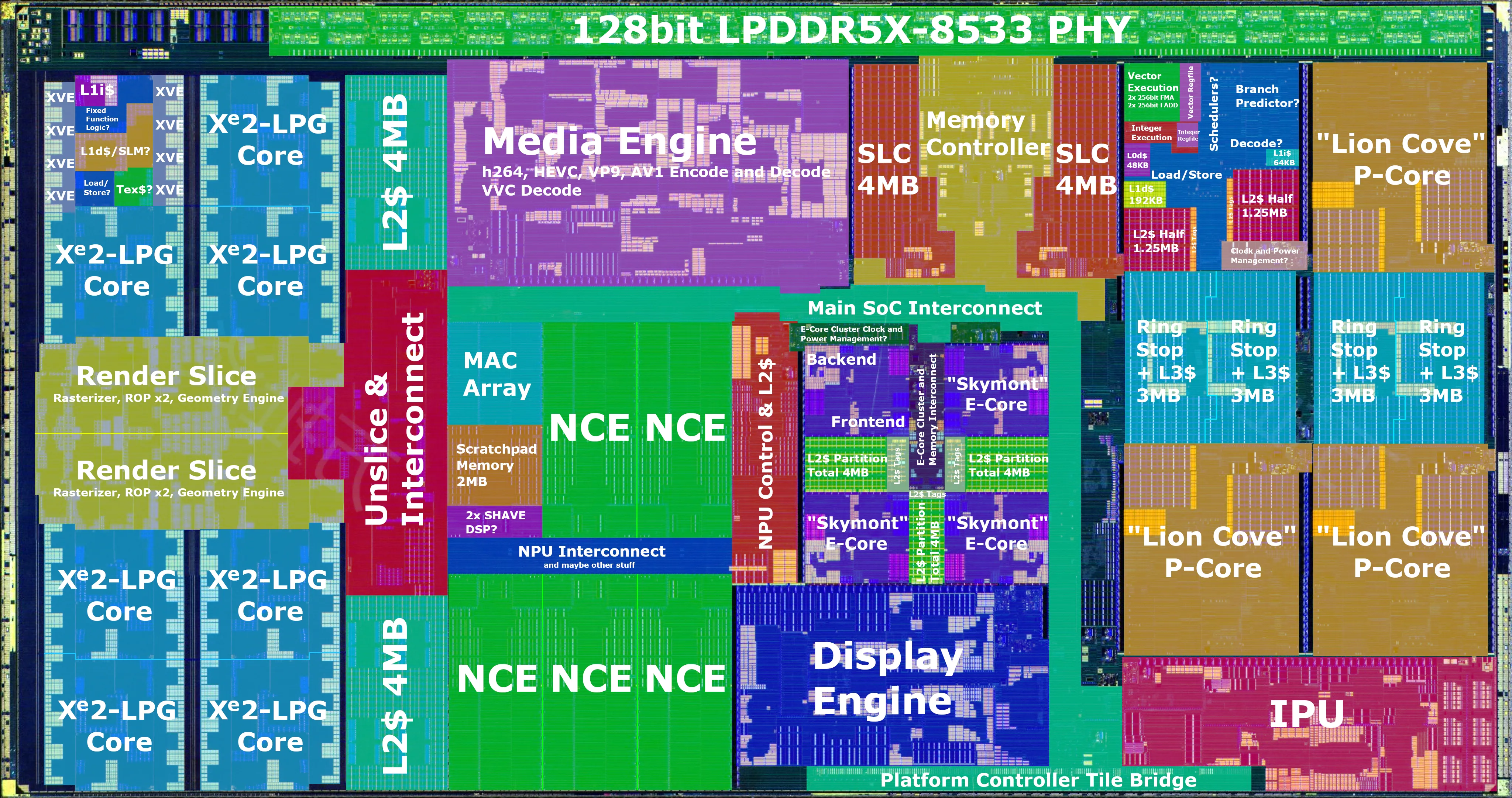 LunarLake Compute Tile
The LunarLake Compute Tile is a chiplet containing the majority of LunarLake-MX, that includes 4 P-Cores, 4 E-Cores, iGPU, NPU, Media and Display engines and the memory controller with SLC.
Annotated View (4096x2162) Download (1008.54 kiB)
Original Source: GeekerWan and 万扯淡, provided by Kurnal.
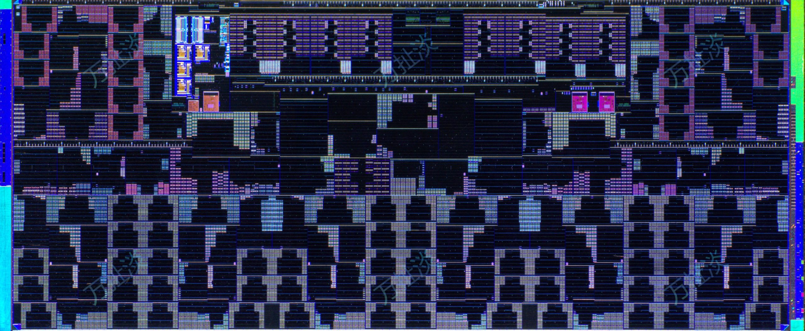
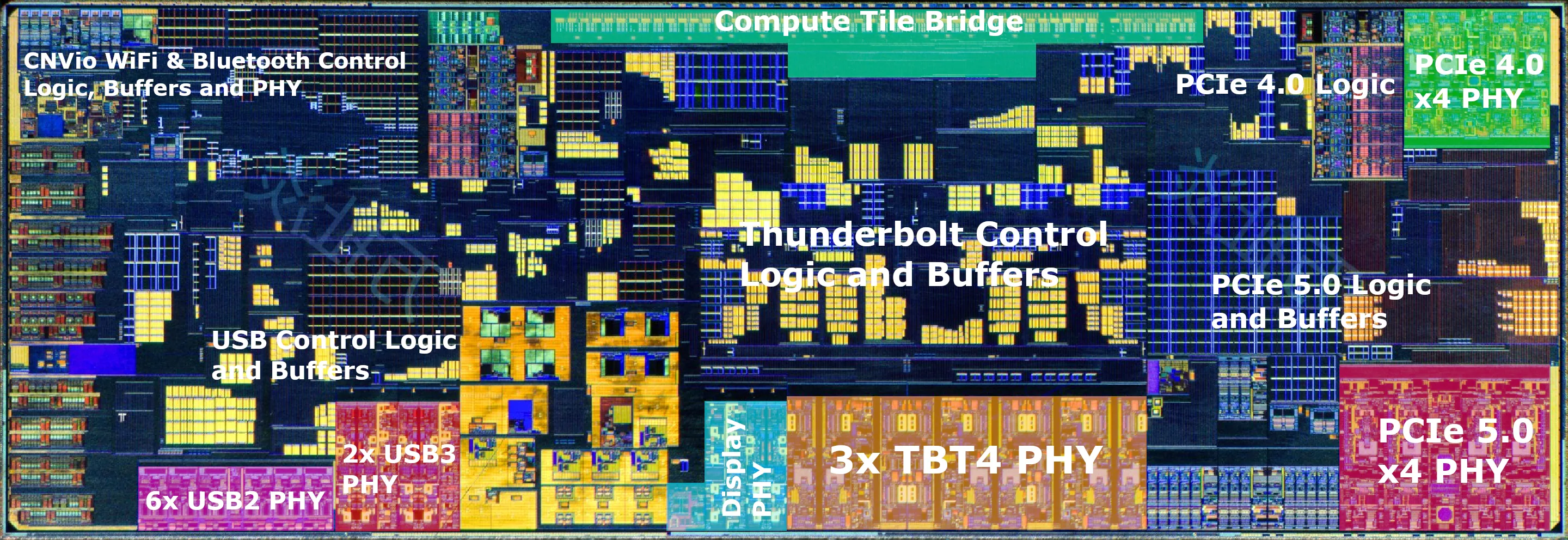 LunarLake Platform Controller Tile
The LunarLake Platform Controller Tile is a chiplet containing most of the I/O of LunarLake-MX, namely USB, Thunderbolt, PCIe, CNVio and miscellaneous low speed platform I/O.
Annotated View (2880x991) Download (583.2 kiB)
Original Source: GeekerWan and 万扯淡, provided by Kurnal.
Intel MeteorLake Architecture
 MeteorLake-P (6+8 Mockup)
The MeteorLake-P multi-chip was used for the first generation Intel Core Ultra series products
This chip utilizes 4 chiplets stacked atop an interposer, split into an SoC tile, supplemental I/O tile, CPU compute tile and a graphics tile.
CPU: 2 or 6 RedwoodCove P-cores, 8 Crestmont E-cores and 2 Crestmont LPE-Cores
GPU: 4 or 8 Xe-LPG Cores (512 or 1024 SIMD lanes)
Memory: 128 bit DDR5-5600/LPDDR5-7467 memory controller
IO: 8 PCIe 5.0 lanes, 20 PCIe 4.0 lanes
Annotated View (13000x6470) Download (3.91 MiB)
Original View (2048x1020) Download (211.92 kiB)
Original Source: QQ, reposted by HXL (9550pro) on Twitter
 MeteorLake Compute Tile
The MeteorLake Compute Tile is a chiplet containing 2 or 6 RedwoodCove P-cores and 8 Crestmont E-Cores alongside 12 or 16 MiB of L3 shared cache.
Annotated View (2106x1281) Download (661.65 kiB)
Original View (2106x1281) Download (776.45 kiB)
Original Source: QQ, reposted by HXL (9550pro) on Twitter
 MeteorLake Graphics Tile
The MeteorLake Graphics Tile is a chiplet containing 4 or 8 Xe-LPG cores split in two Render Slices backed by a 4 MiB L2 cache.
Annotated View (2560x1055) Download (448.38 kiB)
Original View (2560x1055) Download (654.68 kiB)
Original Source: QQ, reposted by HXL (9550pro) on Twitter
 MeteorLake SoC Tile
The MeteorLake SoC Tile is a chiplet containing the memory controller, media engine, display engine, NPU, I/O and also 2 Crestmont LPE-cores with a 2 MiB L2 cache.
Annotated View (2186x2560) Download (1.12 MiB)
Original View (2560x2186) Download (1.34 MiB)
Original Source: QQ, reposted by HXL (9550pro) on Twitter
 MeteorLake I/O Tile
The MeteorLake I/O Tile is a small chiplet containing some of the higher speed I/O such as PCIe 5.0 and Thunderbolt 4 alongside extra lower speed PCIe 4.0 lanes.
Annotated View (2560x749) Download (417.82 kiB)
Original View (2560x749) Download (511.37 kiB)
Original Source: QQ, reposted by HXL (9550pro) on Twitter
Intel RaptorLake Architecture
 RaptorLake-S
The RaptorLake-S chip was used for the upper half of the 13th gen Core series products.
CPU: 8 RaptorCove P-cores and 16 Gracemont E-cores with a shared 36 MiB L3 cache
GPU: 32 Gen12 Execution Units (512 SIMD lanes)
Memory: 128 bit DDR4-3200/DDR5-5600 memory controller
IO: 16 PCIe 5.0 lanes, 4 PCIe 4.0 lanes
Annotated View (20329x11357) Download (106.43 MiB)
Original View (20329x9357) Download (124.88 MiB)
Original Source: Frizchens Fritz (Flickr, Twitter)
 RaptorCove Core
The RaptorCove core was used for RaptorLake-S based products and it is mostly just a higher clocked GoldenCove core with more L2 cache.
Annotated View (9744x18733) Download (87.57 MiB)
Original View (9744x18733) Download (111.36 MiB)
Original Source: Frizchens Fritz (Flickr, Twitter)
 Gracemont Core Cluster
The Gracemont core cluster consists of 4 Gracemont cores and a shared L2 cache.
It was used in the AlderLake and RaptorLake products, with the latter having a larger shared L2 cache.
Annotated View (10351x12645) Download (64.96 MiB)
Original View (10351x11145) Download (76.45 MiB)
Original Source: Frizchens Fritz (Flickr, Twitter)
Intel AlderLake Architecture
 AlderLake-S
The AlderLake-S chip was used for the 12th gen Core series products.
It was also Intel's first large-scale hybrid core design.
CPU: 8 GoldenCove P-cores and 8 Gracemont E-cores with a shared 30 MiB L3 cache
GPU: 32 Gen12 Execution Units (512 SIMD lanes)
Memory: 128 bit DDR4-3200/DDR5-4800 memory controller
IO: 16 PCIe 5.0 lanes, 4 PCIe 4.0 lanes
Annotated View (6950x3514) Download (22.49 MiB)
Original View (6950x3514) Download (24.04 MiB)
Original Source: Intel AlderLake press release
Intel RocketLake Architecture
 RocketLake-S
The RocketLake-S chip was used for the 11th gen desktop Core series products.
Using the CypressCove core which was a SunnyCove core 'backported' to the 14nm manufacturing process.
CPU: 8 CypressCove cores with a shared 16 MiB L3 cache
GPU: 32 Gen12 Execution Units (512 SIMD lanes)
Memory: 128 bit DDR4-3200 memory controller
IO: 20 PCIe 4.0 lanes
Annotated View (21036x10177) Download (133.23 MiB)
Original View (21036x10177) Download (157.01 MiB)
Original Source: Frizchens Fritz (Flickr, Twitter)
Intel Skylake Architecture
 Skylake-X
The Skylake-X chip was used for the 1st generation Xeon Scalable server and Xeon W workstation products.
CPU: 28 Skylake-X cores with a shared 38.5 MiB L3 cache
GPU: None
Memory: Two 192 bit DDR4-2666 memory controllers
IO: 48 PCIe 3.0 lanes
Annotated View (27665x18546) Download (176.16 MiB)
Original View (27665x18546) Download (146.34 MiB)
Original Source: Frizchens Fritz (Flickr, Twitter)

Intel KnightsLanding Architecture
 Knights Landing
The KnightsLanding chip was part of the Xeon Phi line of accelerators/processors, originally derived from project Larrabee. These served as high core count PCIe add-in cards which were later expanded to fit into on-board CPU sockets.
CPU: 76 Knights Landing cores with each cluster of two cores sharing a 1 MiB L2 cache
GPU: None
Memory: Two 192 bit DDR4-2400 memory controllers and eight MCDRAM controllers
IO: 40 PCIe 3.0 lanes
Annotated View (27549x18218) Download (193.1 MiB)
Original View (27549x18218) Download (143.15 MiB)
Original Source: Frizchens Fritz (Flickr, Twitter)
AMD Zen 5 Architecture
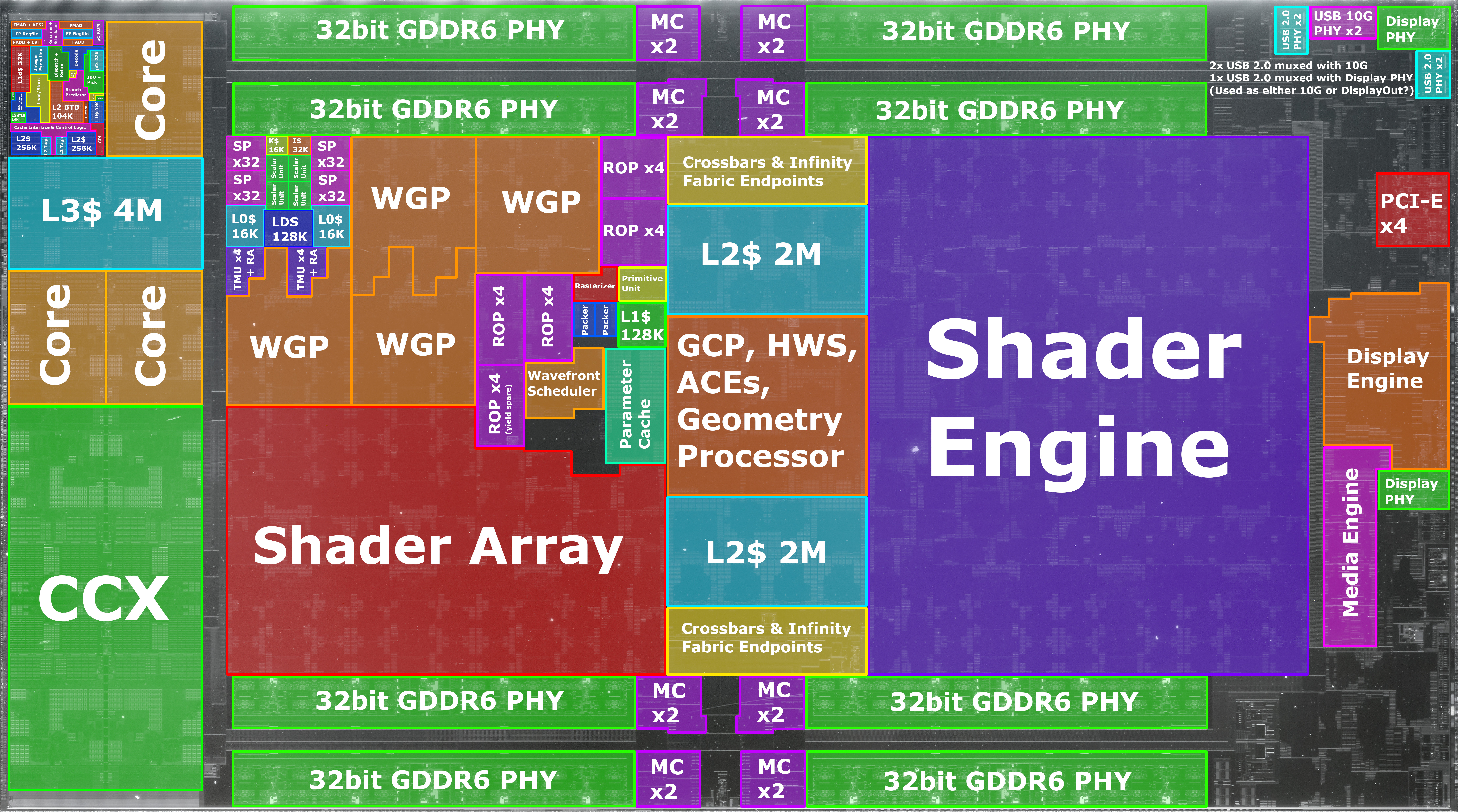
 GraniteRidge
GraniteRidge is the desktop variant of Zen 5, using up to two 8-Core CCDs and the same client IO die as Zen 4 "Raphael".
Annotated View (8681x8678) Download (5.51 MiB)
Original View (2652x2651) Download (590.86 kiB)
Original Source: Frizchens Fritz (Flickr, Twitter)
 Zen 5 CCD
The Zen 5 CCD is a core chiplet containing just CPU cores and cache. It was used in Ryzen 9000 and EPYC 9005 series products.
The chip contains an octa-core Zen 5 core complex with 32 MiB of L3 cache. Additionally it supports an extra L3 'V-Cache' chiplet to be vertically stacked on top of the CCD.
Annotated View (31493x27018) Download (193.68 MiB)
Original View (31493x27018) Download (261.23 MiB)
Original Source: Frizchens Fritz (Flickr, Twitter)
 Zen 5 Core
The Zen 5 core as used by the Ryzen 9000 and EPYC 9005 series products.
Note that this version is different to the Zen 5 cores in mobile StrixPoint CPUs, those have their vector units halved.
Annotated View (10995x5478) Download (11.13 MiB)
Original View (10995x5478) Download (17.19 MiB)
Original Source: Frizchens Fritz (Flickr, Twitter)
 GraniteRidge cIOD
The client desktop Ryzen 7000 and Ryzen 9000 I/O chiplet.
Annotated View (10868x8380) Download (22.21 MiB)
Original View (10868x8380) Download (31.58 MiB)
Original Source: Frizchens Fritz (Flickr, Twitter)
 StrixHalo
The StrixHalo APUU is AMD's mobile workstation SoC based on a chiplet Zen 5 CPU and a big RDNA3.5 iGPU supported by both Infinity Cache and a very wide LPDDR5X interface.
The chip contains up to 16 Zen 5 cores with a total of up to 64 MiB of L3 cache, an RDNA3.5 based iGPU with 20 WGPs, a Xilinx AIE based NPU and is supported by a 256-bit LPDDR5X memory interface backed by 32 MiB of MALL (Infinity Cache).
Annotated View (27959x23708) Download (47.33 MiB)
Original Source: ASUS Tony 俞元麟 and 万扯淡, provided by Kurnal.
 StrixHalo CCD
The StrixHalo CCD differs from the standard Zen 5 CCD by swapping the GMI3 interface with a "raw" link to the IOD using an InFO oS/InFO RDL high density substrate.
Annotated View (5718x4686) Download (5.45 MiB)
Original View (6154x5042) Download (5.63 MiB)
Original Source: ASUS Tony 俞元麟 and 万扯淡, provided by Kurnal.
 StrixHalo IOD
The StrixHalo IO die houses the gigantic 20 WGP RDNA3.5 iGPU, alongside a Xilinx AIE based NPU, dual media engines and a wide 256-bit LPDDR5X memory interface alongside 32 MiB of MALL, known under the marketing name Infinity Cache.
Annotated View (11920x9956) Download (23.9 MiB)
Original View (11920x9956) Download (19.7 MiB)
Original Source: ASUS Tony 俞元麟 and 万扯淡, provided by Kurnal.
 StrixPoint
The StrixPoint APU is AMD's high-end Zen 5 based mobile processor powering the Ryzen AI 300 series.
The chip contains 4 Zen 5 and 8 Zen 5C cores with a total of 24 MiB of L3 cache, an RDNA3.5 based iGPU containing 8 WGPs and a second generation Xilinx AIE based NPU.
Annotated View (4887x3156) Download (4.53 MiB)
Original View (1629x1052) Download (920.25 kiB)
Original Source: QQ, reposted by 포시포시 (harukaze5719) on Twitter
AMD Zen 4 Architecture
 Zen 4 CCD
The Zen 4 CCD is a core chiplet containing just CPU cores and cache. It was used in Ryzen 7000 and EPYC 9004 series products.
The chip contains an octa-core Zen 4 core complex with 32 MiB of L3 cache. Additionally it supports an extra 64 MiB L3 'V-Cache' chiplet to be vertically stacked on top of the CCD for a total of 96 MiB of L3 cache.
Original View (9010x5818) Download (69.63 MiB)
Original Source: Frizchens Fritz (Flickr, Twitter)
 Zen 4 Core
The Zen 4 core as used by the Ryzen 7000 and EPYC 9004 series products.
A "compact" version of this core using dense manufacturing libraries can also be found in the EPYC 97x4 "Bergamo" server processors.
Annotated View (9143x4320) Download (19.73 MiB)
Original View (42990x20313) Download (190.65 MiB)
Original Source: Frizchens Fritz (Flickr, Twitter)
AMD Zen 3 Architecture
 Zen 3 CCD
The Zen 3 CCD is a core chiplet containing just CPU cores and cache. It was used in Ryzen 5000, Ryzen Threadripper 5000 and EPYC 7003 series products.
The chip contains an octa-core Zen 3 core complex with 32 MiB of L3 cache. Additionally it supports an extra 64 MiB L3 'V-Cache' chiplet to be vertically stacked on top of the CCD for a total of 96 MiB of L3 cache.
Original View (39718x26181) Download (193.02 MiB)
Original Source: Frizchens Fritz (Flickr, Twitter)
 Zen 3 Core
The Zen 3 core as used by the Ryzen 5000, Ryzen Threadripper 5000 and EPYC 7003 series products.
A refined version of this core can also be found in the Ryzen 6000 mobile products under the codename 'Zen 3+'.
Annotated View (9526x5489) Download (14.11 MiB)
Original View (9526x5489) Download (15.51 MiB)
Original Source: Frizchens Fritz (Flickr, Twitter)
AMD Zen 2 Architecture
 Zen 2 CCD
The Zen 2 CCD is a core chiplet containing just CPU cores and cache. It was used in Ryzen 3000, Ryzen Threadripper 3000 and EPYC 7002 series products.
The chip contains two quad-core Zen 2 core complexes with 16 MiB of L3 cache each for a total of 8 cores and 32 MiB of L3 cache
Original View (36183x25714) Download (186.19 MiB)
Original Source: Frizchens Fritz (Flickr, Twitter)
 Zen 2 Core
The Zen 2 core as used by the Ryzen 3000, Ryzen Threadripper 3000 and EPYC 7002 series products.
A cut-down version of this core can also be found in the PlayStation 5 console.
Annotated View (3840x2543) Download (18.61 MiB)
Original View (8264x5472) Download (76.17 MiB)
Original Source: Frizchens Fritz (Flickr, Twitter)
 Matisse cIOD
The client IO die of Zen 2 was used in the Ryzen 3000 desktop products codenamed 'Matisse'.
This IO die was also used as the X570, TRX40 and WRX80 chipsets.
CCD IO: Up to 2 CCDs can be connected to the cIOD.
Memory: 128 bit DDR4-3200 memory controller
IO: 32 PCIe 4.0 lanes physically present
Annotated View (11586x8645) Download (36.06 MiB)
Original View (11586x8645) Download (141.67 MiB)
Original Source: Frizchens Fritz (Flickr, Twitter)
 Rome sIOD
The server IO die of Zen 2 was used in the Ryzen Threadripper and EPYC 7002 products codenamed 'CastlePeak' and 'Rome' respectively.
CCD IO: Up to 8 CCDs can be connected to the sIOD.
Memory: Four 128 bit DDR4-3200 memory controllers
IO: 128 PCIe 4.0 lanes, 2 PCIe 3.0 lanes
Annotated View (24460x13327) Download (217.67 MiB)
Original View (24460x13327) Download (185.15 MiB)
Original Source: Frizchens Fritz (Flickr, Twitter)
 Renoir
The Renoir APU was primarily used in Ryzen 4000 series mobile products.
CPU: Two quad-core Zen 2 core complex with 4 MiB of L3 cache each
GPU: 8 Vega Compute Units (512 SIMD lanes) with 512 kiB of L2 cache
Memory: 128 bit DDR4-3200/LPDDR4-4266 memory controller
IO: Max 24 PCIe 3.0 lanes
Annotated View (4241x3360) Download (19.91 MiB)
Original View (4241x3360) Download (6.92 MiB)
Original Source: Frizchens Fritz (Flickr, Twitter)
AMD Zen 1 Architecture
 Zeppelin
AMD's main chip of the Ryzen 1000, Ryzen Threadripper 1000 and EPYC 7001 series.
CPU: Two quad-core Zen 1 core complexes with 8 MiB of L3 cache each
GPU: None
Memory: 128 bit DDR4-2933 memory controller
IO: 32 PCIe 3.0 lanes
Annotated View (19700x8660) Download (58.62 MiB)
Original View (19700x8660) Download (130.63 MiB)
Original Source: Frizchens Fritz (Flickr, Twitter)
 Raven Ridge
Mainstream APU, primarily seen in the Ryzen 2000 mobile line of products but also the Ryzen 3 2200G and Ryzen 5 2400G desktop products.
CPU: Qual-core Zen 1 core complex with 4 MiB of L3 cache
GPU: 11 Vega Compute Units (704 SIMD lanes) with 1 MiB of L2 cache
Memory: 128 bit DDR4-2933 memory controller
IO: Max 16 PCIe 3.0 lanes
Annotated View (10461x5945) Download (30.93 MiB)
Original View (10461x5945) Download (105.87 MiB)
Original Source: Frizchens Fritz (Flickr, Twitter)
 Raven2
A low end APU, primarily seen in the Athlon line of products such as the Athlon 3000G.
CPU: Dual-core Zen 1 core complex with 4 MiB of L3 cache
GPU: 3 Vega Compute Units (192 SIMD lanes) with 512 kiB of L2 cache
Memory: 128 bit DDR4-2933 memory controller
IO: Max 10 PCIe 3.0 lanes
Annotated View (4000x3624) Download (4.09 MiB)
Original View (4000x3624) Download (14.58 MiB)
Original Source: Frizchens Fritz (Flickr, Twitter)
NVIDIA Ada Architecture
 AD102
AD102
The AD102 chip which was used in the high end GeForce RTX 40 series products. Starting with the GeForce RTX 4090.
Core: 144 SMs (18432 SIMD lanes) with 96 MiB of L2 cache.
Memory: 384 bit GDDR6X memory subsystem
IO: 16 PCIe 4.0 lanes
Annotated View (7309x8264) Download (74.43 MiB)
Original View (7309x8264) Download (41.55 MiB)
Original Source: Frizchens Fritz (Flickr, Twitter)
NVIDIA Ampere Architecture
 GA102
GA102
The GA102 chip was used in the high end GeForce RTX 30 series products. Starting with the GeForce RTX 3080.
Core: 84 SMs (10752 SIMD lanes) with 6 MiB of L2 cache.
Memory: 384 bit GDDR6X memory subsystem
IO: 16 PCIe 4.0 lanes, 6 display outputs
Annotated View (7402x8471) Download (13.29 MiB)
Original View (7402x8471) Download (52.15 MiB)
Original Source: Frizchens Fritz (Flickr, Twitter)
NVIDIA Turing Architecture
 TU102
TU102
The TU102 chip was used in the GeForce RTX 2080 Ti and Titan RTX products.
Core: 72 SMs (4608 SIMD lanes) with 6 MiB of L2 cache.
Memory: 384 bit GDDR6 memory subsystem
IO: 16 PCIe 3.0 lanes, 5 display outputs
Annotated View (5074x6367) Download (7.7 MiB)
Original View (5074x6367) Download (29.65 MiB)
Original Source: Frizchens Fritz (Flickr, Twitter)
 TU106
TU106
The TU106 chip was used in the GeForce RTX 2060 and 2070 series of products.
Core: 36 SMs (2304 SIMD lanes) with 4 MiB of L2 cache.
Memory: 256 bit GDDR6 memory subsystem
IO: 16 PCIe 3.0 lanes, 5 display outputs
Annotated View (7640x5835) Download (10.31 MiB)
Original View (7640x5835) Download (64.06 MiB)
Original Source: Frizchens Fritz (Flickr, Twitter)
 TU116
TU116
The TU116 chip was used in the GeForce GTX 16 series products.
Core: 24 SMs (1536 SIMD lanes) with 1.5 MiB of L2 cache.
Memory: 192 bit GDDR6 memory subsystem
IO: 16 PCIe 3.0 lanes, 5 display outputs
Annotated View (7025x4024) Download (6.94 MiB)
Original View (7025x4024) Download (41.64 MiB)
Original Source: Frizchens Fritz (Flickr, Twitter)
NVIDIA Pascal Architecture
 GP100
GP100
The GP100 chip was used in the Tesla P100 and Quadro GP100 products.
Core: 56 SMs (3584 SIMD lanes) with 4 MiB of L2 cache.
Memory: 4096 bit HBM2 memory subsystem
IO: 16 PCIe 3.0 lanes, 6 display outputs
Annotated View (7055x8613) Download (41.6 MiB)
Original View (7055x8613) Download (43.67 MiB)
Original Source: Frizchens Fritz (Flickr, Twitter)
 GP102
GP102
The GP102 chip was used in the GeForce GTX 1080 Ti and Titan X series of products.
Core: 30 SMs (3840 SIMD lanes) with 3 MiB of L2 cache.
Memory: 384 bit GDDR5X memory subsystem
IO: 16 PCIe 3.0 lanes, 6 display outputs
Annotated View (10993x8835) Download (185.01 MiB)
Original View (10993x8835) Download (94.21 MiB)
Original Source: Frizchens Fritz (Flickr, Twitter)
AMD RDNA2 Architecture
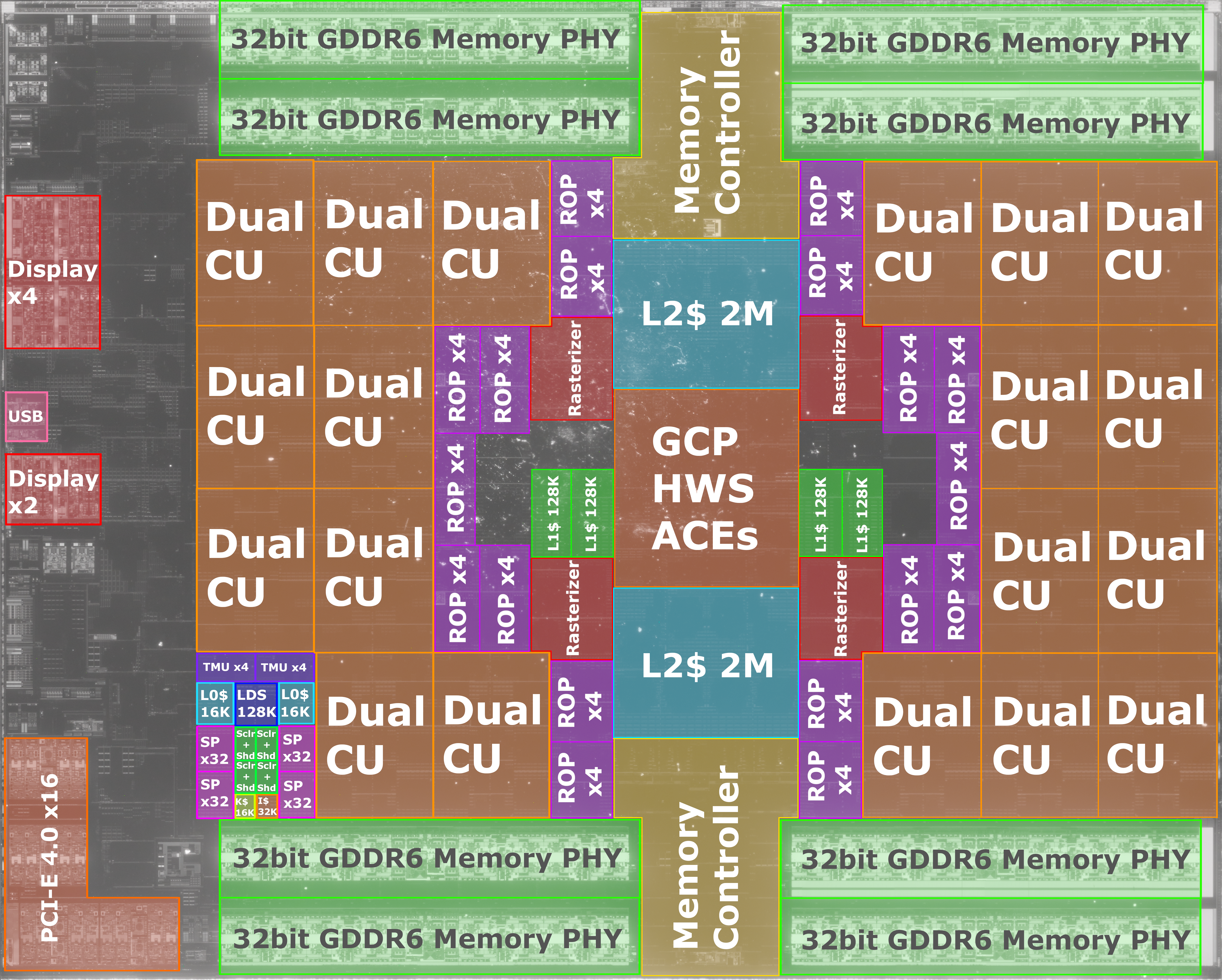
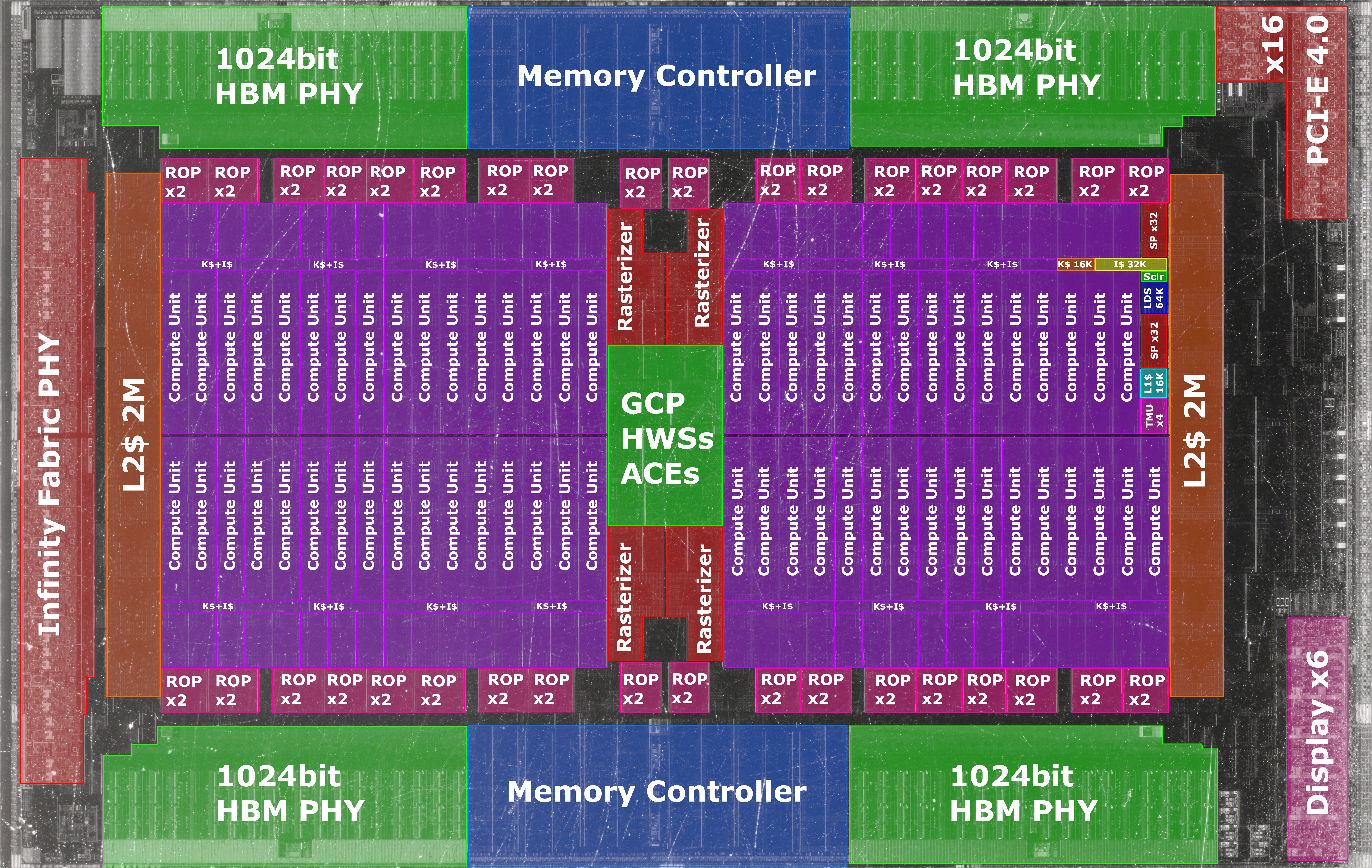
 NAVI21
The Navi 21 chip was used in the ultra-high end Radeon RX 6000 series products.
Core: 40 WGPs (5120 SIMD lanes) with 128 MiB of L3 and 4 MiB of L2 cache.
Memory: 256 bit GDDR6 memory subsystem
IO: 16 PCIe 4.0 lanes, 6 display outputs
Annotated View (2188x1374) Download (878.6 kiB)
Original View (2188x1374) Download (450.69 kiB)
Original Source: Anonymous Source
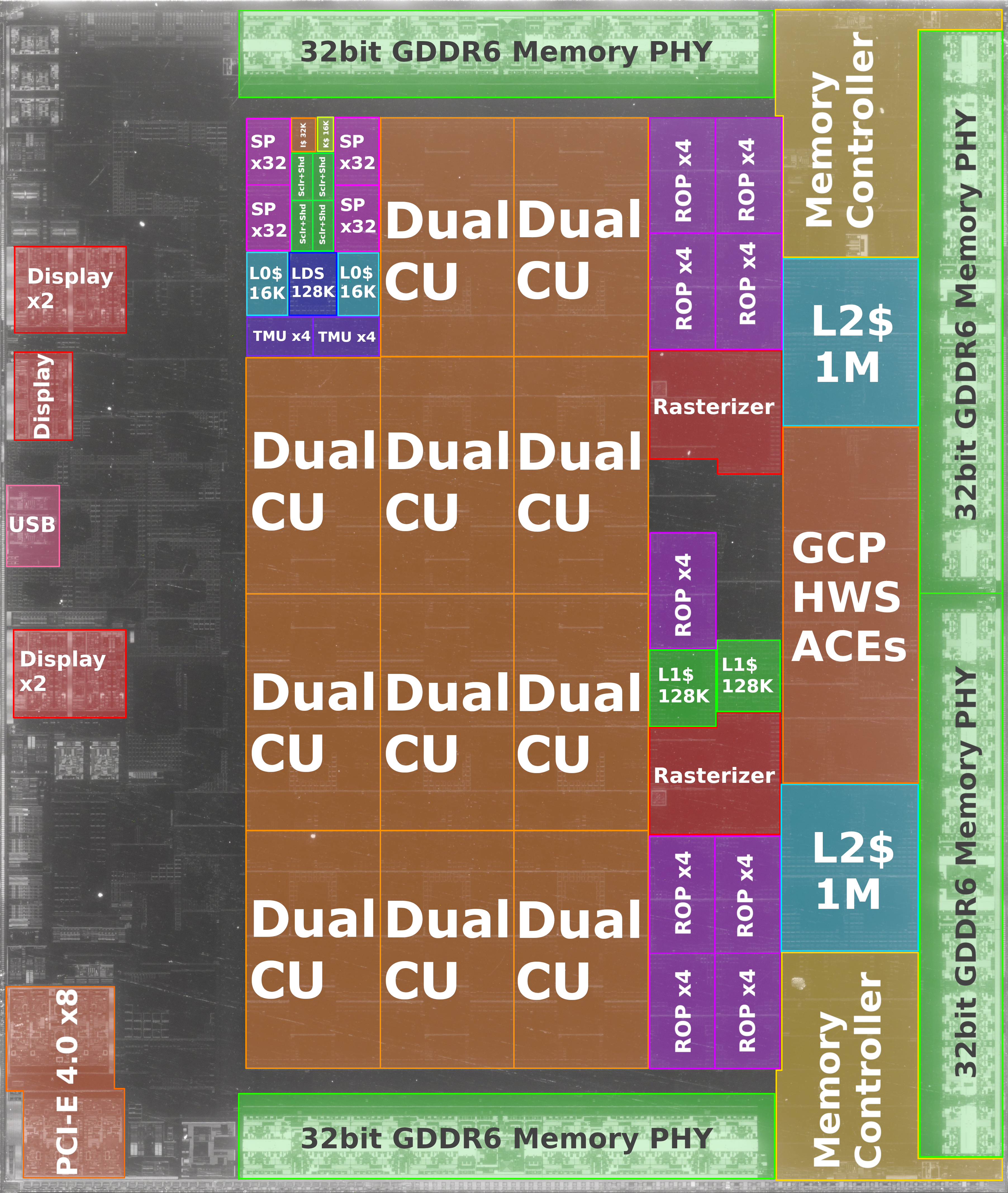
 NAVI22
The Navi 22 chip was used in the high end Radeon RX 6000 series products.
Core: 20 WGPs (2560 SIMD lanes) with 96 MiB of L3 and 3 MiB of L2 cache.
Memory: 192 bit GDDR6 memory subsystem
IO: 16 PCIe 4.0 lanes, 6 display outputs
Annotated View (5740x5730) Download (10.98 MiB)
Original View (5740x5730) Download (23.8 MiB)
Original Source: Frizchens Fritz (Flickr, Twitter)
AMD RDNA1 Architecture
 NAVI10
The Navi 10 chip was used in the high end Radeon RX 5000 series products.
Core: 20 WGPs (2560 SIMD lanes) with 4 MiB of L2 cache.
Memory: 256 bit GDDR6 memory subsystem
IO: 16 PCIe 4.0 lanes, 6 display outputs
Annotated View (5529x4435) Download (33.49 MiB)
Original View (5529x4435) Download (20.29 MiB)
Original Source: Frizchens Fritz (Flickr, Twitter)
 NAVI14
The Navi 14 chip was used in the low end Radeon RX 5000 series products.
Core: 12 WGPs (1536 SIMD lanes) with 2 MiB of L2 cache.
Memory: 128 bit GDDR6 memory subsystem
IO: 8 PCIe 4.0 lanes, 5 display outputs
Annotated View (3608x4270) Download (22.47 MiB)
Original View (3608x4270) Download (14.38 MiB)
Original Source: Frizchens Fritz (Flickr, Twitter)
AMD Vega 20 Architecture
 VEGA20
The Vega 20 chip was used in the datacenter Instinct MI25, workstation Radeon Pro VII and consumer Radeon VII products.
Core: 64 Compute Units (4096 SIMD lanes) with 4 MiB of L2 cache.
Memory: 4096 bit HBM2 memory subsystem
IO: 16 PCIe 4.0 lanes, 6 display outputs
Annotated View (7162x4532) Download (47.63 MiB)
Original View (7162x4532) Download (32.08 MiB)
Original Source: Frizchens Fritz (Flickr, Twitter)
Sony PlayStation 5 System
 PlayStation 5
The PlayStation 5 console from Sony uses a custom SoC made by AMD.
It uses a custom Zen 2 core with a cut-down FPU and custom RDNA graphics.
CPU: Two quad-core Zen 2 core complexes with 4 MiB of L3 cache each
GPU: 20 RDNA WGPs physically (2560 SIMD lanes, 18 WGPs active)
Memory: 256 bit GDDR6 memory subsystem
IO: 4 PCIe 4.0 lanes, 2 display outputs
Annotated View (7233x4028) Download (6.57 MiB)
Original View (7233x4028) Download (26.55 MiB)
Original Source: Frizchens Fritz (Flickr, Twitter)
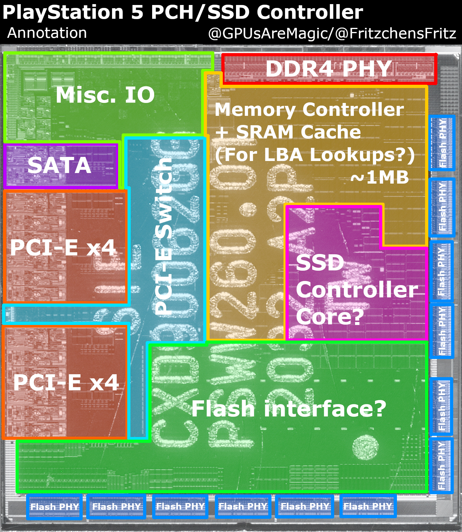 PlayStation 5 Chipset
The PlayStation 5 chipset provides the main SoC access to the user-accessible NVMe slot and SATA optical drive in addition to being the internal SSD controller.
Annotated View (1576x1814) Download (1.28 MiB)
Original View (1576x1664) Download (2.98 MiB)
Original Source: Frizchens Fritz (Flickr, Twitter)
Microsoft Xbox One X System
 Xbox One X
The Xbox One X console from Microsoft uses a custom SoC made by AMD.
It uses the Jaguar core and custom GCN graphics.
CPU: Two quad-core Jaguar core complexes with 2 MiB of L2 cache each
GPU: 44 GCN CUs physically (2816 SIMD lanes, 40 CUs active)
Memory: 384 bit GDDR5 memory subsystem
IO: 8 PCIe 3.0 lanes, 1 display output
Annotated View (20280x13720) Download (135.74 MiB)
Original View (20280x13720) Download (178.6 MiB)
Original Source: Frizchens Fritz (Flickr, Twitter)